Teaching
Resources
Shaping And Slicing Of Germanium Boules Using Wire-Electron Discharge Machining (EDM) For Reduced Subsurface Damage And Increased Productivity
Ph.D. project of Dinesh Rakwal
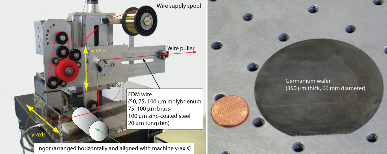
This project seeks to create innovation resulting in the potential use of wire-EDM in the shaping of germanium boules and its subsequent slicing into wafers. This method promises the potential of decreased subsurface damage at the edge of the wafers, which is thought to be the leading cause for wafer breakage during handling and a principal cause of latent defects in the orbiting solar cell applications. A second benefit of the proposed machining process is the potential for better flatness of the wafers, which allows the wafers to be cut thinner compared to conventional methods, while simultaneously reducing the amount of material to be removed to achieve the required flatness. A third advantage of wire-EDM is the fact that the wire used in the process (25-50 μm diameter) is significantly thinner than the diamond-coated wire currently in use (150 μm). This allows considerably more wafers to be cut from s single boule, thereby increasing the production yield and decreasing manufacturing cost. Using wire-EDM to shape the boule and slice the wafers has a fourth, potentially very beneficial aspect: Most excess material removed is in the form of large pieces which have a better potential for recoverability compared to the dust that is produced with conventional, abrasive machining processes. If performed economically, this "green" process will reduce waste and further reduce manufacturing cost.
Germanium wafers have a similar lattice constant as gallium arsenide (GaAs), making it a perfect substrate for GaAs-based multi-junction solar cells which are used on virtually all U.S. space-based defense, civil and commercial satellites. As such, multi-junction solar cells are considered to be a defense-critical technology that requires the establishment of a U.S. domestic capability to fabricate the precision germanium substrates critical to multi-junction cell fabrication. However, current production of germanium wafers suffers from extremely poor yield. This is, in large, due to the fact that Ge-production processes were designed for use with Si manufacturing in mind. Germanium, however, is considerably more brittle than silicon, causing a noticeable portion of the wafers to break during handling, heating, and other fabrication processes. It is widely believed that the cylindrical grinding which is required to shape the boule to its final diameter, introduces damage below the machined surface. This subsurface damage, which can easily extend 50-70 microns into the material, triggers microcracking along the edge of the wafer. These cracks propagate as a result of stresses that occur during handling, causing the wafer to fracture catastrophically.
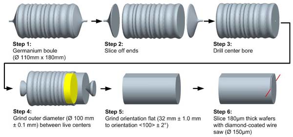
Conventional boule shaping through cylindrical grinding and wafer slicing with a wire saw:
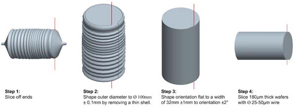
Proposed technique: Wire-EDM for shaping and Slicing:
Publications:
D. Rakwal, E. Bamberg (in press). Slicing, cleaning and kerf analysis of germanium wafers machined by wire electrical discharge machining. Journal of Materials Processing Technology. DOI: 10.1016/j.jmatprotec.2008.08.027. Published online on September 4, 2008.
E. Bamberg, D. Rakwal (2008). Experimental investigation of wire electrical discharge machining of gallium-doped germanium. Journal of Materials Processing Technology 197, pp. 419-427.
D. Rakwal, E. Bamberg (2007). Using Taguchi methods to optimize the slicing rate and surface roughness for wire electrical discharge machining of p-type germanium. In: Proc. 15th International Symposium on Electromachining (ISEM XV), Pittsburgh, PA, April 23-27, 2007, pp. 127-132.
C. Orino, D. Rakwal, J.D. Jorgensen, E. Bamberg (2006). Development of a precision, low-cost, small footprint wire electron discharge machine (WEDM). In: Proc. 2006 ASPE Conf., Monterey, CA, October 15-20, 2006, (26), pp. 239-242.