Teaching
Resources
Precision Design Laboratory
Welcome to the homepage of the Precision Design Lab (PDL) at the University of Utah. The lab is part of the Department of Mechanical Engineering and is located in the Merrill Engineering Building (MEB) at the northern end of the Salt Lake City campus. Under the guidance of Prof. Eberhard Bamberg, undergraduate and graduate students conduct research in the areas of precision design, micro machining, and biomedical instrumentation.
Research Spotlight 1:
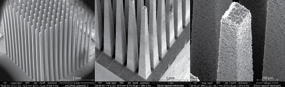
High-aspect ratio fabrication of silicon microelectrode arrays with micro electrical discharge machining
High electrode count neural interfaces are an essential tool in understanding and learning about the central and peripheral nervous system of animals and humans. Monolithically fabricated devices from silicon thus far were limited to electrode lengths of around 1.5 mm. This limits the area of cortical sulci to be interfaced with.
Using micro wire electrical discharge machining (micro-WEDM), the electrodes with lengths of up to 9 mm were machined successfully. A method of etching to remove the recast layer was also investigated. Source: Rakwal et al (in press).
Figure 1: Silicon microelectrode array with 144 tapered electrodes. The electrode length is 5 mm. The recast layer shown in the left image will be removed later through chemical etching.
Research Spotlight 2:
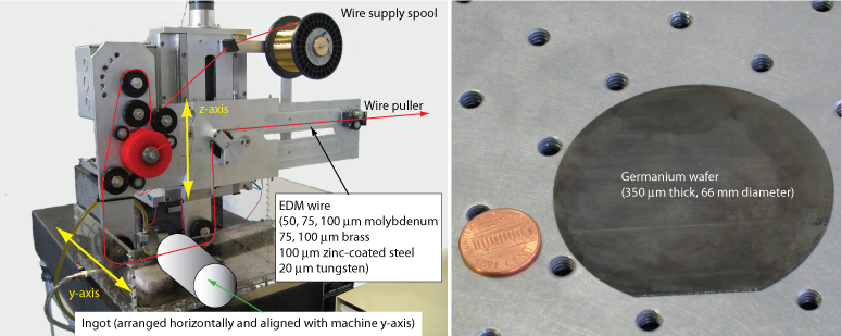
Slicing of germanium wafers with wire electrical discharge machining
Germanium, like many other semiconducting materials, is extremely brittle and prone to micro cracking as a result of mechanical stresses from abrasive processes such as boule grinding and wafer slicing with wire saws. Wire electrical discharge machining (WEDM) was sucessfully used to slice wafers of 300 micron thickness without any detectable micro cracks.
Another advantage of WEDM is the fact that thin EDM wires (100 micron diameter or less) produce a significantly reduced kerf compared to wire saws. This reduces the amount of material wasted during the slicing, thereby lowering the cost per wafer. more>>
Figure 2: Prototype WEDM for slicing semiconductor wafers (left). Germanium wafer sliced with WEDM (right)
There are those who look at things the way they are, and ask why... I dream of things that never were, and ask why not?
Robert Francis Kennedy, 1968 presidential campaignAddress:
Precision Design Lab
Department of Mechanical Engineering
50 South Central Campus Drive, 2124 MEB
Salt Lake City, UT 84112
Fax (801) 585-9826